System & Board Level Design
Acronics provides a complete and comprehensive turnkey design solution for board level designs. Specializing in high speed design and layout technologies, we have developed boards for systems with data rates up to 40 gigabits per second.
Design and Schematic Capture
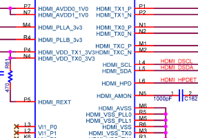
Using state-of-the-art EDA design tools, Acronics’ engineers can take the design specification, select appropriate components and develop the corresponding schematics. A bill of materials is provided early in the design cycle so that component ordering can take place.With in-house developed tools, we can connect large pin-count elements like FPGA/ASIC devices quickly and accurately. Symbol/Geometry generation is also provided if required. Using in-house tools, our engineers have the capability to generate these directly from datasheets, thus greatly minimizing the probability for entry errors.
Signal Integrity
Interconnections between devices such as dense BGA and RAM devices at high speeds and edge rates are no longer a trivial connectivity issue. In addition to this, running these high speed signals through connectors can be a daunting task without the introduction of signal degradation and crosstalk.Acronics employs best practice techniques for the simulation of high-speed transmission lines incorporating I/O, PCB and connector models to the required degree of accuracy. This in turn leads to the use of appropriate layout, termination, and tracking methods to guarantee success on first power up. Signal Integrity Analysis can also be performed where less than ideal layout and tracking is warranted, to evaluate the performance of signals under these conditions.

PCB Manufacture and Assembly
System/Board Level Functional Simulation
Acronics provides our customers with quality PCBs at the very competitive pricing by working with our strategic PCB partners in the U.S. and overseas including Taiwan, China, South Korea and Vietnam.
Acronics provides:
- State-of-the-Art SMT PCB Assembly
- Fast turnaround prototype boards
- High volume capability
- Low cost solutions
- Highest Quality solutions and products
In some instances, it is advantageous to functionally simulate the full board or part of the board at the system level. Modeling is an extremely effective way to verify the functionality and connectivity. In general, a judgment must be made early, as to whether the effort required to develop models to fill any “gaps” is cost effective and beneficial. Acronics can help in the development of the board level simulation and components modeling.
Impedance Controlled Layout
Design for Test
Acronics engineers can suggest an optimal layer stack up, board material and trace width/spacing. This ensures that any critical impedance requirements will be met and that the PCB will be routable and met EMC requirements. Acronics has considerable experience in designing reliable multi-gigahertz PCB layouts which achieve the lowest possible EMI/RFI radiation.
Logic Analyzer headers and strategic test-points to facilitate testing, boundary scan chain hook-up and scan clock distribution, and LED indicators are all measures regularly employed by Acronics to ensure a high degree of testability for system boards.